Tuesday 30 April 2013

The HTSSOP and Altium

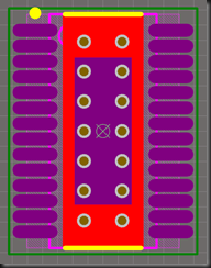
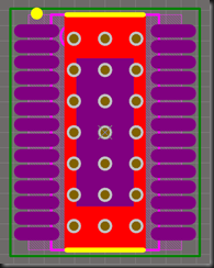
After reviewing several land-pattern options for my HTSSOP-28 'PowerPAD' Plastic Small Outline package TLC5940, I've decided to use the one from the chip's datasheet. The datasheet made many references to the SLMA002 and SLMA004 application notes, but the key points I got from both of these were to:
  • use as much copper and as many vias as possible to facilitate heat transfer, and
  • tent the vias to prevent solder wicking away from the chip
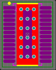
To the first point, the SLMA002 version has ten vias, while the example footprint in the chip's datasheet uses twenty-one. Secondly, tenting directly below the chip's thermal pad would be a nightmare as I'm trying to get as large of a soldering contact area as possible. So with those observations, I've decided to use the land-pattern shown in the datasheet (Fig.2 below, purple being the inverse of the solder mask, red the masked copper).
00 01 AM
Fig.1: SLMA002 Recommended
Fig.2: TLC5940 Datasheet
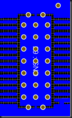
Fig.3: A Colleague’s footprint
Figure 3 shows a footprint for a different TI chip with the same package (SN65HVS880), but with:
  • different land-pattern than the example recommended in the datasheet, and
  • a strange, asymmetrical via pattern
The first point may be the result of several things, such as an out-dated datasheet, but regardless, as I said, I’ve made my decision to go with Figure 2.
Thanks go to Scott for demonstrating how to specify the polygon-connect style for individual pads on a specific footprint:
  1. Add a new design rule to ‘Design -> Design Rules -> Plane -> Polygon Connect Style’
  2. Specify the first ‘object’ to be a solution to the query: ‘IsPad AND Name = 'U1-29'‘; where ‘U1’ is the name of the chip, and ‘29’ is the specific pad number we would like to pour across.
  3. Watch Altium correctly pour the polygon across specified pad and be happy.
relief direct
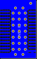
Fig.4: Before Scott
Fig.5: After Scott
Notice the thermal relief in Figure 4 and the solid connection in Figure 5. I've added four extra vias to the PCB (and probably hinder hand-soldering... eeep) to promote vertical heat transfer due to the abundance of physical space. Anyway, let’s get this baby off to the manufacturer!

Saturday 27 April 2013

3D Component Models for PCAs

I've been messing around with embedded software for the last few weeks, but lately my time's been dominated by linking some proper 3D models to my PCA for accurate component clearance checking.

The key areas I was unsure about with my current design were:

  • Through-hole LEDs
  • Through-hole connectors
  • Surface-mount capacitors
  • Surface-mount fasteners

The LED-to-fastener conflict had a chance to be a game-changer, so I decided to 'do things right' by using the tools available to me; a combination of Altium and SolidWorks.
A lot of the models I used were readily available for free on various manufacturer websites and forums, which made short work of a lot of it. Some that I've used are:

  • Texas Instruments - Their data appears very accurate, although a couple of their web-links are broken and I've asked for them to be fixed.
  • TE Connectivity - Excellent 3D models for connectors, but without colour in the one I used.
  • PEM Fasteners - Again, great models, but with some colour 'issues'.
  • http://www.3dcontentcentral.com - The Dassault Systèmes (makers of SolidWorks) website for anyone to upload free components.

I downloaded all my passive 'chip' components (resistors, capacitors, inductors) from 3D Content Central, and a couple of ICs too, but most of the ICs I got from Texas Instruments, although as I said, one of their links for the HTSSOP28 chip was broken, so I've substituted a TSSOP28 (no thermal pad... not that it matters from a purely visual point of view) for the TLC5940s (I can't remember if I noted previously that I've switched from the through-hole to one of the surface-mount variants for reasons of cost).
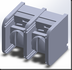
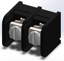
The model for the PEM Fasteners SMD threaded-nut I've purchased came with an orange colour on the threading which may be to highlight that a) the threading wasn't modelled, or b) that it is a contact surface, but I didn't want it to look unrealistic, so I changed it to silver. The Tyco barrier-terminal model came without any colour information, which I suspected may have been due to them using an older .STEP file format, but it appears to be a STEP AP214 format which should have colour options. This became a simple matter of using SolidWorks to import the file, add the colour to the appropriate surfaces, and save as an updated .STEP model, as shown below in the before and after images:

tyco001 tyco002

Figure 1: Connector before adding colour

Figure 2: Connector with colour

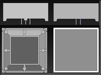
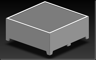
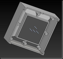
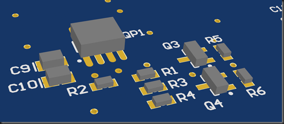
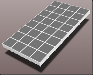
The first component I had to make from scratch was the tri-colour LED that is placed in an array across the entire top-side of the board. I didn't have great technical documentation for the 'internals' of the component, so my digital callipers came in handy. Previously I had modelled the component as a single flat-block, but this caused clashes with one bottom-layer component (the Tyco barrier-connector) and one top-layer component (the SMD fastener). While I knew I could probably get away with an educated-guess as a valid position where the components wouldn't collide, it's always better to be sure.

RoyalFourWay001 RoyalIso002 RoyalIso001

Figure 3: LED Front/Side/Bottom/Top

Figure 4: LED Iso Above

Figure 5: LED Iso Below


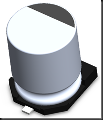
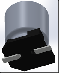
The second component was the KEMET EDK-Series SMD 16V, 470uF electrolytic capacitor. This provided some more good design 'revision' with SolidWorks (which I haven't touched in over a year). It was a relatively simple component to model, and I found that when I needed to revise one of the dimensions I'd set early on, the method I'd used to link my 'Smart Dimensions' - as they're called - meant that the model was automatically realigned and adjusted for the change. Handy!

KemetFourWay001 KemetIso001 KemetIso002

Figure 6: Kemet from all angles

Figure 7: Kemet Iso Above

Figure 8: Kemet Iso Below


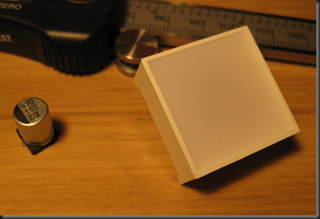
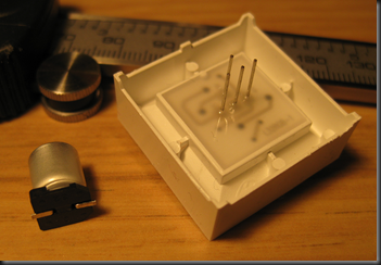
And here are those two components in real life in their natural environment:

realLEDCap001 realLEDCap002

Figure 9: Capacitor right, LED Left

Figure 10: Capacitor right, LED Left


So with all the components modelled, I was able change the layout from this:

PCBold001 PCBold002

Figure 11: Leadless-components

Figure 12: Missing Connectors


...to this:

PCB003 PCB000

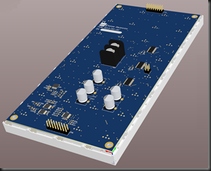
Figure 13: Front

Figure 14: Back

PCB005 PCB006

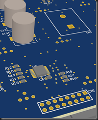
Figure 15: ICs and colourful 'jellybeans'

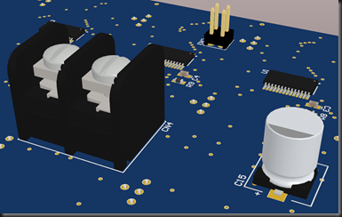
Figure 16: Barrier Terminal, header pins, capacitor


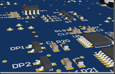
Now that all the components are spatially accurate, I can see that there is no longer a problem with clashes between components:

PCBold003 Edit PCB004

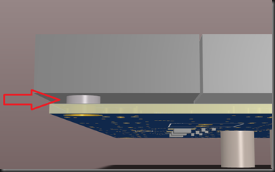
Figure 17: Fastener has tight fit

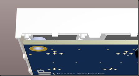
Figure 18: Spacious fastener

One thing to note is that I have the footprint for the electrolytic capacitor slightly larger than necessary so that I can temporarily use a few larger 35V 470uF capacitors that I acquired cheaply.
Hopefully I'll get the board off to the manufacturer tomorrow. It's always best to sleep on a design and re-check for design faults in the morning; a 'cooling-off period'. :)

Monday 8 April 2013

LEDs Received?!

I'm not sure why I received this package today, but it seems to contain 1,540 RBG LEDs (420 shown, pen and tip-of-toe shown for scale). Did anyone mistakenly ship these to me?


I guess I'll just put them into storage until the owner comes forward.

Sunday 7 April 2013

STM32 System and Timer Clock Configurations - Pt2

Now that I've verified my system's core clock is functioning as expected, I can move onto configuring the clock modules to produce the desired BLANK and GSCLK signals to control the TLC5940 chips.

Using the SYSCLK signal, the 'Advanced High-performance Bus' (AHB) clock frequency is set via a prescaler. In this case I am using the maximum frequency of the AHB by setting the prescaler to divide by 1. The two 'Advanced Peripheral Bus' clocks (APB1 and APB2) are generated from the AHB via their associated prescalers. They have maximum frequencies of 42 and 84MHz respectively, so my APB1 prescaler is set to '4' and APB2 prescaler is set to '2'. The internal signal that can be selected as the timer peripherals' clock is the APB1 clock.

HOWEVER... and this is an important part to take note of: While the APB1 signal provides the clock for numerous peripherals including the timer modules, the timers can receive a faster clock if the APB1 prescaler is set to anything other than '1'. The manual states:
  1. If the APB prescaler is 1, the timer clock frequencies are set to the same frequency as that of the APB domain to which the timers are connected.
  2. Otherwise, they are set to twice (×2) the frequency of the APB domain to which the timers are connected.
Since the APB1 prescaler I am using is '4' and the AHB clock is 168MHz, the internal clock presented to the timer modules is actually (168/4) * 2 = 84MHz. Inside the TIMx modules there are three main clock signals:
  • CK_INT - The internal clock before prescaling
  • CK_PSC - The clock signal after being divided by the prescaler
  • CK_CNT - The counter clock, which generates pulses every time the prescaler counter overflows
Note that while there are different clock signals (internal clock, external clock, internal triggers, etc) that can be used as the main input to each timer module, since I don't need to synchronise to external signals, I will use the default internal clock, APB1. The internal clock signal APB1 is fed into my main timer module TIM3. This module will be used to provide both the GSCLK signal on an external GPIO pin, and also to trigger/clock the slave TIM4 module which will provide the BLANK pulses. Initially I intend to have the TIM3 setup for its fastest possible rate, and then configure the output for the desired GSCLK frequency once both signals are synchronised correctly. I am using a prescaler divide factor of 1 (TIM3_PSC = 0), so CK_PSC = CK_INT = APB1 * 2 = 84MHz.

Each TIM module from TIM2 to TIM5 (and some others) can be used as a 'master' or a 'slave' to generate signals or react to them in various ways. For instance, I can use TIM3 as a master that generates a trigger pulse every time the counter reaches a specific value. I could then use that trigger pulse as the main clock signal in another timer module.

The way I intend to use TIM3 is to use its 'Update Event' as its external trigger signal (TRGO) which generates a single pulse every time its counter 'overflows', or reaches the upper limit which is set in the 'Auto Reload Register' (ARR). The TIM3 counter is configured in 'Upcounter Mode' which means that every rising edge of the counter clock causes the counter to increment until it reaches the ARR value. When it reaches this upper limit, it generates an 'Update Event', UEV, which causes the counter to reset to '0'. Each UEV pulses the trigger signal, so if ARR is set to '1', the counter moves from 0 to 1, generates a trigger pulse, resets the counter to 0, and the process repeats forever.

This two-count overflow acts as a divide-by-two on the CK_CNT signal. Therefore, our TIM3 master trigger signal is 84MHz / 2 = 42MHz.

This trigger is passed into TIM4 on the Internal Trigger network, which, when these two specific timers are used, is the Internal Trigger 2 signal (ITR2).

Returning to the original task of providing grayscale clock and blanking pulse signals for the TLC5940, the two timer modules now need to be configured to generate these signals on their Output Compare pins.

For the GSCLK signal, the TIM3 Output Compare Channel 1 (OC1) signal is configured to toggle its output every time the counter matches the desired value; in this case '1'. This essentially means that it is synchronised with the TRG0 signal at half the frequency.

For the BLANK signal, we need to be able to synchronise the signals with a phase shift so that the desired number of GSCLK pulses are generated before a blanking pulse is generated. To do this, the TIM4 counter is configured in 'Centre Aligned' mode, so that it counts up to the ARR value and then counts down to zero and repeats. The TIM4 OC1 signal is configured as a PWM signal that is set when the counter is less than OC1's  Capture/Compare Register (CCR1) value, where:
  • CCR1 = GSCLK_COUNT + 1
Due to internal timing, the TIM3 OC1 signal is given a slight phase shift relative to the TIM4 OC1, and the result is that the number of rising edges between consecutive blanking pulses is the desired number (GSCLK_COUNT). I'm still not exactly sure why, so I'll need to investigate the origin of this phase shift, but for now I am happy that it's there.

The timing for each timer module, and the resulting signals seen by the TLC5940 chip are shown below in Fig.1. Here GSCLK_COUNT is set to '2'. Note that for TIM4, the CK_INT is TIM3's TRG0.

Figure 1: TIM3, TIM4, and the TLC5940 Signal Configuration

I've experimented with changing the TIM3 prescaler to adjust the GSCLK frequency, different numbers of GSCLK_PULSES. Below Fig. 2 and Fig. 3 show scope captures of two different configurations:

Figure 2: GSCLK = 21MHz, GSCLK_COUNT = 2
Figure 3: GSCLK = 82kHz, GSCLK_COUNT = 4

Now that the timing of the TLC5940 GSCLK and BLANK signals have been configured and are easily adjustable for the desired frequency and intensity resolution, it's time to move onto the TLC5940's serial data interface.
Wednesday 3 April 2013

STM32 System and Timer Clock Configurations - Pt1

I've started writing some software to drive a series of TLC5940 16 Channel LED Driver chips on an ST STM32F407 Microcontroller. I previously had code working on an Atmel microcontroller, but obviously with the change of hardware comes the need for re-writing some of the lower peripheral configuration and application code.

The two main requirements for driving the TLC5940 chip from a microcontroller are:
  1. The grayscale clock
  2. A serial data bus
The microcontroller's SPI port is well suited to delivering data to the TLC5940 even though this is not officially an 'SPI' device. For the grayscale clock I have decided to use the STM32's timer modules to automatically provide the BLANK and GSCLK signals.

Basically, the blank signal is used to reset the grayscale counter inside the TLC5940, and depending on the desired LED brightness resolution, we wait a certain number of GSCLK cycles before generating a BLANK pulse to reset the TLC5940's internal counter.

Both these signals have timing requirements placed on them, so we need to understand exactly how the STM32's timer modules function. And before we can do this, we also need to understand the clock source that drives the timers (in my case, the internal system clock).

My board uses an external 8MHz crystal oscillator as its clock source, and although I believed I had it configured correctly, bit without measuring it, I couldn't be sure. Well... I could have flashed an LED at a human-measurable speed, like 1Hz, but that's not as fun as delving right into the core and working out to the timer modules. :p

The maximum frequency specified by ST for this device is 168MHz, so this is the frequency I will configure the device for. To begin with, the 8MHz clock is the 'High Speed External' clock signal, or HSE as it is known, enters the microcontroller through its OSC_IN/OSC_OUT pins, before being sent to the 'Phase Lock Loop' (PLL) module to be divided and multiplied by several pre-scalers to provide the 'System Clock' (SYSCLK), the 'Advanced High-performance Bus' (AHB) clock, and the two 'Advanced Peripheral Bus' clocks (APB1 and APB2). There are several other clocks configured by the 'Reset and Clock Control' (RCC) peripheral, but these aren't directly related to the Timer modules I am using.

The C source files in the STM32F4xxStdPeriph Library where the system clock is configured include:
  • system_stm32f4xx.c - the PLL register value #DEFINEs and initialisation code is found here
  • stm32f4xx.h - the HSE frequency is defined at the start
The SystemCoreClock variable in the first of the two files above is calculated using the following two equations found in the RM0090 Reference Manual:
  • f(VCO clock) = f(PLL clock input) × (PLLN / PLLM)
  • f(PLL general clock output) = f(VCO clock) / PLLP
These equations describe what is happening in the hardware. First, the HSE clock signal is divided by the PLLM division factor. The result from this must be between 1 - 2MHz, but a value of 2MHz is recommended to limit PLL jitter.
This pre-scaled signal then enters the Main PLL module where it is multiplied by PLLN, the VCO multiplication factor, to provide a signal between 64 to 432MHz, and then divided back down by the PLLP factor to produce the SystemCoreClock with a frequency no greater than 168MHz.

My initial setup used the following configuration:

stm32f4xx.h:
  • #define HSE_VALUE    ((uint32_t)8000000)
system_stm32f4xx.c
  • #define PLL_M      8
  • #define PLL_N      336
  • #define PLL_P      2
However after noticing the mention of increased clock jitter, I decided to change PLL_M to '4', PLL_N to '168'. All the PLL parameters above are placed into the 'RCC PLL Configuration Register', RCC_PLLCFGR.

Now, with the settings for the core clock determined and initialised into code, I needed a way to view these signals, and luckily for me the nice people at ST have provided hardware that can select from various internal clock signals, pre-scale them, and present them for viewing on two external pins, MCO1 and MCO2 which are the 'Microcontroller Clock Output' pins. These are configured in the 'RCC Clock Configuration Register' RCC_CFGR using the MCOx bits for selecting the desired signal, and the MCOxPRE bits to scale the signal by a factor of between 1 and 5.

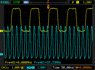
Using the peripheral library commands below, I've selected the HSE for MCO1, and SYSCLK divided by 5 for MCO2. This should provide signals of 8MHz and 33.6MHz if my configuration is correct.
  • RCC_MCO1Config(RCC_MCO1Source_HSE, RCC_MCO1Div_1);
  • RCC_MCO2Config(RCC_MCO2Source_SYSCLK, RCC_MCO2Div_5);
And viewing these signals in the images below we can see that this is roughly the case. The 0.8% error in the SYSCLK (blue Ch2) signal is either due to the actual signal being slightly out due to the PLL scaling system, or possibly the limitations of my cheap 100MHz 'scope (I will test this tomorrow on some old (but high-end) Le Croy and Tektronix 500MHz 'scopes at work tomorrow.


Next I'm moving on to confirming my GSCLK and BLANK timer configuration is as I need it to be.

UPDATE:

I've taken some measurements with the scopes at work and they appear to agree with the 8MHz result, but definitely show the 33.6MHz SYSCLK (within the margin of error):