The two main requirements for driving the TLC5940 chip from a microcontroller are:
- The grayscale clock
- A serial data bus
The microcontroller's SPI port is well suited to delivering data to the TLC5940 even though this is not officially an 'SPI' device. For the grayscale clock I have decided to use the STM32's timer modules to automatically provide the BLANK and GSCLK signals.
Basically, the blank signal is used to reset the grayscale counter inside the TLC5940, and depending on the desired LED brightness resolution, we wait a certain number of GSCLK cycles before generating a BLANK pulse to reset the TLC5940's internal counter.
Both these signals have timing requirements placed on them, so we need to understand exactly how the STM32's timer modules function. And before we can do this, we also need to understand the clock source that drives the timers (in my case, the internal system clock).
My board uses an external 8MHz crystal oscillator as its clock source, and although I believed I had it configured correctly, bit without measuring it, I couldn't be sure. Well... I could have flashed an LED at a human-measurable speed, like 1Hz, but that's not as fun as delving right into the core and working out to the timer modules. :p
The maximum frequency specified by ST for this device is 168MHz, so this is the frequency I will configure the device for. To begin with, the 8MHz clock is the 'High Speed External' clock signal, or HSE as it is known, enters the microcontroller through its OSC_IN/OSC_OUT pins, before being sent to the 'Phase Lock Loop' (PLL) module to be divided and multiplied by several pre-scalers to provide the 'System Clock' (SYSCLK), the 'Advanced High-performance Bus' (AHB) clock, and the two 'Advanced Peripheral Bus' clocks (APB1 and APB2). There are several other clocks configured by the 'Reset and Clock Control' (RCC) peripheral, but these aren't directly related to the Timer modules I am using.
The C source files in the STM32F4xxStdPeriph Library where the system clock is configured include:
- system_stm32f4xx.c - the PLL register value #DEFINEs and initialisation code is found here
- stm32f4xx.h - the HSE frequency is defined at the start
The SystemCoreClock variable in the first of the two files above is calculated using the following two equations found in the RM0090 Reference Manual:
- f(VCO clock) = f(PLL clock input) × (PLLN / PLLM)
- f(PLL general clock output) = f(VCO clock) / PLLP
This pre-scaled signal then enters the Main PLL module where it is multiplied by PLLN, the VCO multiplication factor, to provide a signal between 64 to 432MHz, and then divided back down by the PLLP factor to produce the SystemCoreClock with a frequency no greater than 168MHz.
My initial setup used the following configuration:
stm32f4xx.h:
My initial setup used the following configuration:
stm32f4xx.h:
- #define HSE_VALUE ((uint32_t)8000000)
system_stm32f4xx.c
- #define PLL_M 8
- #define PLL_N 336
- #define PLL_P 2
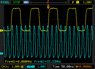
Now, with the settings for the core clock determined and initialised into code, I needed a way to view these signals, and luckily for me the nice people at ST have provided hardware that can select from various internal clock signals, pre-scale them, and present them for viewing on two external pins, MCO1 and MCO2 which are the 'Microcontroller Clock Output' pins. These are configured in the 'RCC Clock Configuration Register' RCC_CFGR using the MCOx bits for selecting the desired signal, and the MCOxPRE bits to scale the signal by a factor of between 1 and 5.
Using the peripheral library commands below, I've selected the HSE for MCO1, and SYSCLK divided by 5 for MCO2. This should provide signals of 8MHz and 33.6MHz if my configuration is correct.
- RCC_MCO1Config(RCC_MCO1Source_HSE, RCC_MCO1Div_1);
- RCC_MCO2Config(RCC_MCO2Source_SYSCLK, RCC_MCO2Div_5);


No comments:
Post a Comment