After reviewing several land-pattern options for my HTSSOP-28 'PowerPAD' Plastic Small Outline package TLC5940, I've decided to use the one from the chip's datasheet. The datasheet made many references to the SLMA002 and SLMA004 application notes, but the key points I got from both of these were to:
- use as much copper and as many vias as possible to facilitate heat transfer, and
- tent the vias to prevent solder wicking away from the chip
To the first point, the SLMA002 version has ten vias, while the example footprint in the chip's datasheet uses twenty-one. Secondly, tenting directly below the chip's thermal pad would be a nightmare as I'm trying to get as large of a soldering contact area as possible. So with those observations, I've decided to use the land-pattern shown in the datasheet (Fig.2 below, purple being the inverse of the solder mask, red the masked copper).
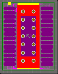 |  |  |
Fig.1: SLMA002 Recommended
|
Fig.2: TLC5940 Datasheet
|
Fig.3: A Colleague’s footprint
|
Figure 3 shows a footprint for a different TI chip with the same package (SN65HVS880), but with:
- different land-pattern than the example recommended in the datasheet, and
- a strange, asymmetrical via pattern
The first point may be the result of several things, such as an out-dated datasheet, but regardless, as I said, I’ve made my decision to go with Figure 2.
Thanks go to Scott for demonstrating how to specify the polygon-connect style for individual pads on a specific footprint:
- Add a new design rule to ‘Design -> Design Rules -> Plane -> Polygon Connect Style’
- Specify the first ‘object’ to be a solution to the query: ‘IsPad AND Name = 'U1-29'‘; where ‘U1’ is the name of the chip, and ‘29’ is the specific pad number we would like to pour across.
- Watch Altium correctly pour the polygon across specified pad and be happy.
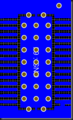 | 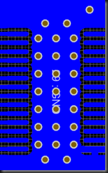 |
Fig.4: Before Scott
|
Fig.5: After Scott
|
Notice the thermal relief in Figure 4 and the solid connection in Figure 5. I've added four extra vias to the PCB (and probably hinder hand-soldering... eeep) to promote vertical heat transfer due to the abundance of physical space. Anyway, let’s get this baby off to the manufacturer!


No comments:
Post a Comment